
Thin HDI PCB Empower Precision Electronics
In today’s world, where smartphones, wearable devices, foldable screens, medical implants, and high-end automotive electronics constantly demand thinner, smaller, and higher-performance solutions, traditional PCBs can no longer meet the dual requirements of “ultra-thin thickness” and “high-density routing.”
Thin HDI PCBs (High-Density Interconnect ultra-thin printed circuit boards) have emerged as the key solution to resolve the contradiction between extreme space compression and high-speed signal transmission.
This article provides a comprehensive breakdown of thin HDI PCBs from definition, core features, manufacturing processes, design considerations, typical applications, to future trends—helping engineers and electronics enthusiasts understand this core technology that underpins precision electronic innovation.
What is a Thin HDI PCB?
HDI (High-Density Interconnect) is a PCB technology that achieves high-density routing through microvias, fine line widths, and tight spacing. Thin HDI PCBs further optimize the substrate and manufacturing process, controlling board thickness in the 0.2mm–0.8mm range (typical HDI boards are ≥1.0mm) while maintaining or even enhancing routing density and electrical performance.
Its key characteristics are: ultra-thin thickness + micro blind/buried vias + fine lines + high integration, solving the problems of traditional thin boards (poor mechanical strength, low routing density) while overcoming the limitations of conventional HDI boards being too thick for ultra-thin devices.
Core criteria:
- Board thickness ≤0.8mm
- Minimum line width/spacing ≤3/3mil (75/75μm)
- Microvia diameter ≤0.15mm
- Extensive use of blind vias, buried vias, and via-in-pad designs
- More efficient interlayer connections and significantly higher space utilization than ordinary thin boards or conventional HDI boards
Core Technical Features of Thin HDI PCBs
Thin HDI is not simply making HDI boards thinner; it is the deep optimization of materials, structure, and process. Its core features include:
Extremely Thin, Maximized Space Utilization
- Board thickness typically 0.2–0.6mm; in some special cases even as thin as 0.15mm—only 1/3–1/5 the thickness of traditional PCBs.
- Blind and buried vias replace conventional through-holes, saving routing space. Routing density can increase by over 30%, allowing tiny boards (fingernail-sized) to integrate chips, sensors, RF modules, and other complex circuits.
Microvia Interconnection, More Flexible Routing
- Uses laser microvias (0.1–0.15mm diameter) with blind and buried via structures:
Blind vias: connect only surface and adjacent inner layers
Buried vias: connect only inner layers, fully hidden within the board
- Reduces signal interference and frees surface routing space, ideal for multi-layer ultra-thin boards—key to achieving “thin but strong.”
Fine Line Width and Tight Spacing, Suitable for Precision SMT
- Achieves 2–3mil line width/spacing, far better than conventional PCBs (5–8mil).
- Perfect for QFN, BGA, CSP, and other fine-pitch ICs, supporting high-precision SMT assembly and small component layouts.
Excellent Electrical Performance, High-Speed and Low-Loss
- Shorter routing, easier impedance control, lower parasitic inductance/capacitance.
- Low signal loss and short delay; impedance deviation controlled within ±8%.
- Ideal for high-frequency, high-speed applications such as 5G, Bluetooth, WiFi, with strong interference resistance.
Lightweight with Structural Resilience
- Thinner boards use less material, reducing overall device weight.
- Coupled with high-toughness ultra-thin substrates (thin FR-4, PI), the board maintains bend resistance and shape stability, suitable for wearables and foldable devices.
Key Manufacturing Processes of Thin HDI PCBs
The manufacturing threshold for thin HDI PCBs is significantly higher than that of conventional PCBs. It requires strict control over equipment precision, processes, and material selection. The key processes include:
Ultra-Thin Substrate Selection
- Priority is given to materials such as high-Tg thin FR-4, ultra-thin Rogers high-frequency materials, and PI (polyimide).
- Typical thickness per layer: 0.05–0.2mm
- Must balance mechanical strength, thermal resistance, and electrical performance
- Prevent warping or cracking during lamination and soldering
Laser Microvia Drilling
- Uses UV laser drilling instead of mechanical drilling
- Enables precise microvias of 0.1–0.15mm diameter
- Smooth via walls and high positional accuracy
- Essential for blind/buried via interconnections
Ultra-Thin Lamination and Thickness Control
- Vacuum lamination ensures precise layer thickness and board flatness
- Prevents warping and delamination in thin structures
- Controlled electroplating ensures uniform copper thickness without affecting overall board thinness
Fine Line Etching and Via-in-Pad Technology
- Advanced etching achieves 2–3mil fine ხაზ (line width/spacing)
- Via-in-pad places microvias directly within pads
- Saves space and improves soldering reliability for packages like BGA
Surface Finishing and Warpage Control
- Common finishes: ENIG (immersion gold), immersion silver, OSP
- Ensures solderability and corrosion resistance
- Strict temperature and humidity control throughout production
- Warpage controlled within 0.5% via leveling and baking processes, ensuring smooth SMT assembly
Advantages Over Standard Thin PCBs and Conventional HDI
| Performance Metric | Thin HDI PCB | Standard Ultra-Thin PCB | Conventional HDI PCB |
| Thickness Range | 0.2–0.8mm | 0.2–0.6mm | 1.0–2.0mm |
| Routing Density | Extremely high (fine lines + microvias) | Low (simple routing only) | High (but thicker) |
| Mechanical Strength | Good, anti-warping | Poor, prone to deformation | Excellent, but heavier |
| High-Frequency Performance | Excellent, low loss | Average, higher interference | Good, but larger size |
| Application Scenarios | Ultra-thin + high-performance devices | Simple low-density devices | Standard high-density devices |
Typical Applications of Thin HDI PCBs
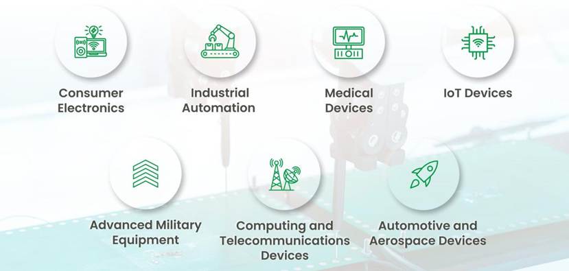
With their ultra-thin and high-density characteristics, thin HDI PCBs are widely used in advanced precision electronics:
Consumer Electronics
Smartphones, foldable phones, smartwatches, TWS earbuds, tablets, etc.
- Example: flagship smartphone motherboards, foldable hinge circuits, smartwatch mainboards
- Typically use 0.3–0.6mm thin HDI
- Reduce device size while increasing battery space and endurance
Medical Electronics
Devices such as pacemakers, endoscopes, micro monitors, and wearable medical devices
- Require extreme miniaturization, reliability, and biocompatibility
- Thin HDI meets strict requirements for implantable and compact medical systems
Automotive Electronics
Sensors, ADAS modules, central control mini boards, in-vehicle cameras
- Must deliver high performance in limited space
- Withstand temperature extremes and vibration
- Thin HDI offers both reliability and compactness
Aerospace and Industrial Control
Satellite modules, drone flight controllers, portable industrial instruments
- Require lightweight, compact, and stable performance
- Thin HDI ensures reliability in harsh environments while reducing weight
Emerging Fields
VR/AR devices, flexible electronics, micro-robots
- Combined with flexible substrates, thin HDI enables curved and bendable designs
- Expands product design possibilities
Design Considerations for Thin HDI PCBs
For engineers, designing thin HDI PCBs requires balancing manufacturability and performance. The following points are critical:
- Control Board Thickness and Layer Count
Avoid blindly pursuing extreme thinness. Balance layer count with mechanical strength. A thickness above 0.3mm is generally recommended for stable mass production yield.
- Prioritize Blind/Buried Vias, Minimize Through-Holes
Use structures like 1+N+1 (outer-layer blind vias + inner buried vias) to reduce through-hole usage and free up routing space.
- Match Impedance and Trace Width
Perform impedance simulations in advance. Fine traces must still meet current-carrying requirements to avoid signal distortion.
- Manage Warpage and Heat Dissipation
Distribute components evenly and reserve thermal paths. Thin boards have poorer heat dissipation, so avoid localized overheating.
- Align with Manufacturer Capabilities
Microvia size, trace width/spacing, and stack-up must match the fabricator’s process capabilities to ensure the design is manufacturable.
Final Thoughts
Thin HDI PCBs are not simply a “slimmed-down PCB,” but a deep integration of high-density interconnect technology and ultra-thin manufacturing processes. They serve as the core carrier enabling lightweight design, high performance, and high integration in advanced precision electronics.
From the smartphone in your pocket to implantable medical devices inside the human body, thin HDI PCBs support continuous innovation in the electronics industry through extreme space efficiency and stable electrical performance.
For hardware engineers, mastering the design and selection of thin HDI PCBs is essential for building compact, high-performance products. As manufacturing processes continue to mature, thin HDI technology will expand into more consumer and industrial applications, becoming one of the dominant directions of the future PCB market.
At the same time, choosing an experienced HDI PCB manufacturer with strong capabilities in ultra-thin processing, microvia technology, and precision fabrication will be critical to ensuring both performance and manufacturability in next-generation electronic designs.