How to Perform Surface Mount SMT Soldering
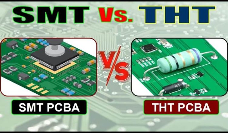
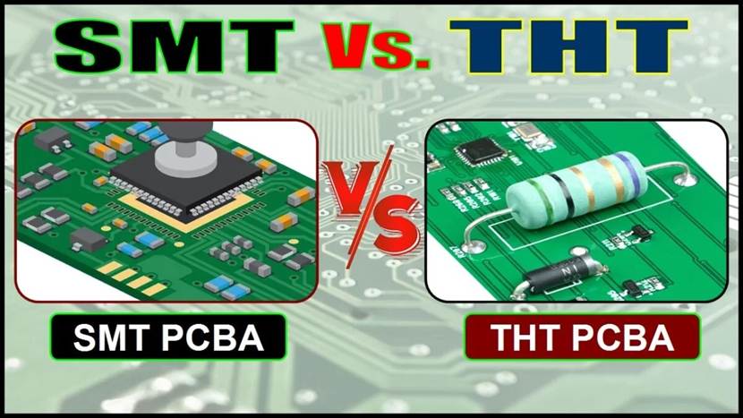
In modern electronics manufacturing, Surface Mount Technology (SMT) has largely replaced traditional through-hole soldering and become the dominant method for PCB assembly. From tiny chips inside smartphones and earbuds to industrial control boards and RF modules, nearly all precision electronic devices rely on surface mount soldering.
Many beginners consider SMT soldering “hard to get into” — components are extremely small, pins are densely packed, and issues like cold joints, solder bridges, or excess solder can easily occur. However, the reality is much simpler: once you understand the standard workflow, proper tools, and essential techniques, you can handle both manual SMD soldering (for prototyping and R&D) and gain a solid understanding of industrial SMT assembly.
This guide provides a comprehensive and practical breakdown of surface mount soldering, including:
- Fundamental concepts
- Essential tools and materials
- Step-by-step manual soldering tutorials
- Industrial SMT production workflow
- Common defects and troubleshooting
- Advanced tips and best practices
Whether you’re a complete beginner or an experienced engineer looking to refine your process, this guide will help you build solid, professional-level soldering skills.
1. What is Surface Mount Soldering (SMT)?
Definition of SMT
Surface Mount Technology (SMT) is a soldering method in which surface mount devices (SMDs) are directly placed onto designated pads on the PCB and soldered using solder paste or molten solder to achieve both electrical and mechanical connections.
The key difference compared to Through-Hole Technology (THT) is:
- SMD components have no leads or very short leads
- Components are mounted directly on the PCB surface
- No drilling is required
This results in several major advantages:
- Smaller size and higher component density
- Better high-frequency performance
- Higher level of automation
- Ideal for modern electronics that demand miniaturization and precision
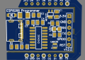
Common Types of SMD Components (by Package)
Understanding component packages is essential before starting soldering. Below are the most common categories:
Passive Components (Chip Components)
Resistors, capacitors, and inductors in packages such as:
- 0402
- 0603
- 0805
The smaller the package, the more challenging the handling and soldering.
Transistors & Diodes
Typical packages include:
- SOT-23
- SOT-89
- SOD-123
These components usually have fewer pins, making them relatively beginner-friendly.
Integrated Circuits (ICs)
Common package types:
- QFP (Quad Flat Package) – gull-wing leads on all four sides
- QFN / DFN (Leadless packages) – pads located underneath
- SOIC (Small Outline IC) – widely used and easier to solder
- BGA (Ball Grid Array) – advanced package with solder balls underneath
As pin density increases, soldering difficulty rises significantly.
Connectors & Sockets
Examples include:
- SMT pin headers
- FPC connectors
These require high placement accuracy and stable solder joints.
Essential Tools and Materials for SMT Soldering
Core Soldering Tools (Must-Have)
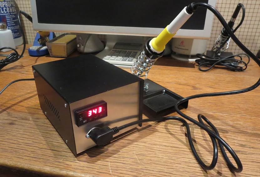
Temperature-Controlled Soldering Iron
- Adjustable temperature range: 250–400°C
- Recommended power: 30–60W
- Tip types: conical (fine tip) and knife (K tip)
- Prefer ESD-safe models to prevent electrostatic damage to ICs
A stable temperature is critical for consistent solder joints.
Soldering Iron Tips
Different tip shapes serve different purposes:
- Fine conical tip (0.2–0.5 mm) → small components & fine-pitch pins
- Knife tip (K tip) → drag soldering for ICs
- Hoof tip → large pads and high thermal mass areas
Using the correct tip dramatically improves efficiency and quality.
Hot Air Rework Station (Hot Air Gun)
A must-have tool for SMT work:
- Used for IC removal and rework (QFP, QFN, BGA, etc.)
- Adjustable temperature and airflow
- Recommended: ESD-safe models
Essential for multi-pin components and rework scenarios.
ESD-Safe Soldering Station (Advanced Option)
- Integrated system (soldering iron + hot air)
- More precise temperature control
- Ideal for frequent or professional use
Auxiliary Tools (Must-Have)
ESD Tweezers
- Types: straight tip / curved tip
- Material: stainless steel
- Used for handling SMD components without damage
Desoldering Tools
- Desoldering braid (wick) → best for fine-pitch pins
- Solder sucker (pump) → quick bulk solder removal
Essential for fixing solder bridges and excess solder.
Flux (Flux Paste / Flux Pen)
- Reduces surface tension
- Removes oxidation
- Greatly improves solder flow and success rate
Highly recommended for beginners — it makes soldering significantly easier.
PCB Holder / Fixture
- Keeps the PCB stable during soldering
- Prevents movement and alignment issues
- Frees both hands for precise work
ESD Protection Equipment
- ESD wrist strap
- ESD mat
Protects sensitive components such as CMOS and RF ICs from electrostatic discharge.
Magnification Tools
- Magnifying glass or digital microscope
Essential for:
- 0402 and smaller components
- Fine-pitch IC inspection
Soldering Consumables (Must-Have)
Solder Wire
- Recommended: Lead-free solder (Sn96.5/Ag3.0/Cu0.5)
- Diameter: 0.3–0.6 mm (thinner is better for SMD work)
- With rosin core (built-in flux, beginner-friendly)
Solder Paste
- Mixture of solder powder + flux
- Used for reflow soldering and batch assembly
- Requires refrigerated storage
Cleaning Solutions
- Isopropyl alcohol (IPA) or PCB cleaner
Removes flux residue to:
- Prevent corrosion
- Maintain electrical performance
Cleaning Materials
- Lint-free wipes
- Cotton swabs
Advanced Tools (Optional – For Professional Use)
For R&D labs, repair centers, or small-scale production:
- Manual pick-and-place machine
- Reflow oven
- Vacuum pickup pen
- BGA rework station
- Infrared thermometer
These tools significantly improve efficiency, consistency, and precision.
Pre-Soldering Preparation — Prevent Failures Before They Happen
Why Preparation Matters
In SMT soldering, up to 80% of failures originate from poor preparation rather than the soldering process itself.
Issues such as cold joints, solder bridges, or component damage are often caused by:
- Contaminated pads
- Oxidized surfaces
- Moisture in components
- Electrostatic discharge (ESD)
Proper preparation is not optional — it is critical for reliable soldering.
ESD Protection (Top Priority)
Electrostatic discharge can instantly damage sensitive components, especially:
- CMOS devices
- RF ICs
- High-density integrated circuits
Basic ESD Safety Practices:
- Wear an ESD wrist strap, properly grounded
- Work on an ESD-safe mat
- Avoid static-generating clothing (e.g., wool, synthetic fibers)
- Always handle components by the body, never touch pins or pads directly
Even a small static discharge can cause latent failures that are difficult to detect.
PCB and Component Pre-Treatment
PCB Inspection

Before soldering, ensure:
- Pads are clean, flat, and free of oxidation
- No oil, dust, or contamination is present
- No pad lifting or physical damage
If oxidation is present:
- Lightly polish with fine sandpaper
- Clean thoroughly with IPA before soldering
Component Inspection
Check all SMD components for:
- Bent or damaged leads/pads
- Oxidation or contamination
- Correct part number, package, and polarity
Pay special attention to:
- Diodes (polarity marking)
- ICs (pin orientation / Pin 1 indicator)
Moisture Control (Pre-Baking)
For components stored in humid environments or for long periods:
- Bake at 80–100°C for 10–15 minutes
This prevents:
- Solder splattering (“popcorning”)
- Internal damage due to moisture expansion during heating
Tool Setup and Calibration
Soldering Iron Temperature
- Lead-free solder: 320–350°C
- Leaded solder: 280–310°C
- Fine-pitch components → use slightly lower temperatures
Hot Air Rework Settings
- Temperature: 300–380°C
- Airflow: Low setting (Level 1–2)
- Distance from PCB: 2–3 cm
Low airflow prevents components from being blown away.
Tip Preparation (Tinning the Tip)
Before starting:
- Heat up the soldering iron
- Apply a small amount of solder to the tip
This:
- Removes oxidation
- Improves heat transfer
- Ensures smooth solder flow
Manual SMT Soldering
To make learning more effective, components are organized from easy to difficult.
Category 1: Passive Components (0402 / 0603 / 0805)
Difficulty: ⭐ (Beginner Level)
Simple structure, usually non-polar — ideal for practice, step-by-step process
1. Secure the PCB
Fix the PCB using a holder to keep it stable and level.
2. Pre-tin One Pad
Apply a small amount of solder to one pad.
Keep it thin and even.
3. Place the Component
Use ESD tweezers to hold the component and align it with the pads.
4. Initial Soldering
Heat the pre-tinned pad while holding the component in place.
Once the solder melts and wets the terminal, remove the iron.
5. Alignment Adjustment
Check if the component is centered.
If misaligned, reheat and reposition.
6. Solder the Second Pad
Apply flux if needed, then solder the opposite side.
7. Cleaning & Inspection
Clean flux residue and inspect the joints:
Smooth, shiny, and properly wetted.
Category 2: Transistors & Diodes (SOT-23, SOD-123)
Difficulty: ⭐⭐
Low pin count, but polarity matters, key steps:
1. Verify Polarity
Diode stripe = cathode
Match PCB silkscreen marking
2. Fix One Pin First
Solder one lead to secure the component.
3. Check Alignment
Ensure correct orientation and positioning.
4.Solder Remaining Pins
Heat each joint ≤ 2 seconds to avoid overheating.
5. Inspection
- No solder bridges
- Smooth joints
- Correct polarity
Category 3: Multi-Pin ICs (SOIC, QFP)
Difficulty: ⭐⭐⭐
Fine-pitch leads — drag soldering is the key technique, step-by-step process
1. Position & Fix the IC
- Pre-tin diagonal pads
- Align the IC with the silkscreen
- Solder opposite corners to secure
Use magnification to ensure perfect alignment.
2. Apply Flux Generously
Coat all pins with a thin, even layer of flux.
More flux = smoother drag soldering.
3. Drag Soldering Technique
- Load a small amount of solder on the tip
- Gently drag along the pins in one direction
Solder will naturally flow to pads and pins.
4. Fix Solder Bridges
If bridging occurs:
- Place desoldering braid over pins
- Heat to absorb excess solder
5. Cleaning & Inspection
Inspect each pin carefully:
- No cold joints
- No bridges
- Even and well-formed solder joints
Category 4: Leadless Packages (QFN / DFN)
Difficulty: ⭐⭐⭐⭐
Hidden pads underneath — requires hot air rework, step-by-step process
1. Pad Preparation
- Apply a thin solder layer to pads
- Add flux to center thermal pad
2. Place the IC
Align carefully with PCB markings using tweezers.
3. Hot Air Soldering
- Set temperature: 320–350°C
- Use low airflow
- Heat evenly around the IC
Stop heating once solder reflows.
4. Cooling
Let it cool naturally for 5–10 seconds
Do not touch or move during this time
5. Inspection
- Use a multimeter for continuity testing
- Ensure proper connection of hidden pads
Category 5: BGA Packages (Advanced Rework)
Difficulty: ⭐⭐⭐⭐⭐ (Professional Level)
Solder balls underneath — requires specialized equipment, basic workflow:
1. Reballing (if needed)
- Clean old solder balls
- Reapply solder balls or use stencil + paste
2. Precise Alignment
- Align BGA with PCB pads
- Use optical alignment if available
3. Reflow Process
- Use a BGA rework station
- Follow proper reflow profile:
Preheat → Soak → Reflow → Cooling
4. Inspection
- Use X-ray inspection
- Check for:
Cold joints
Missing connections
Industrial SMT Assembly Process (Automated Production Line)
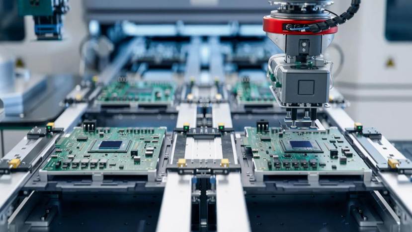
Understanding the industrial SMT workflow not only helps you grasp the principles behind manual soldering, but also provides insight into how high-volume PCB assembly achieves speed, precision, and consistency.
Modern SMT production is highly automated, ensuring:
- High efficiency
- Consistent quality
- Scalable manufacturing
Below is the standard end-to-end SMT production process:
1. Solder Paste Printing
A stainless steel stencil is used to accurately deposit solder paste onto PCB pads.
Key factors:
- Paste volume control
- Alignment accuracy
- Stencil quality
Poor printing is one of the most common sources of defects.
- Pick-and-Place (Component Placement)
High-speed pick-and-place machines:
- Pick SMD components from feeders
- Precisely place them onto solder-pasted pads
Features:
- High placement accuracy (micron-level)
- Extremely fast throughput
- Handles thousands of components per hour
3. Reflow Soldering
The PCB enters a reflow oven, where solder paste melts and solidifies according to a controlled temperature profile:
Preheat → Soak → Reflow → Cooling
This process forms reliable solder joints across all components simultaneously.
4. AOI (Automated Optical Inspection)
AOI systems automatically inspect the PCB for defects such as:
- Cold joints
- Solder bridges
- Misalignment
- Missing components
Ensures early detection before further processing.
5. Rework & Repair
Defective boards are:
- Identified through AOI or manual inspection
- Repaired by skilled technicians using rework stations
Ensures yield and reduces waste.
6. Cleaning & Electrical Testing
Final steps include:
- Cleaning flux residues (if required)
- Functional and electrical testing
Ensures:
- Circuit reliability
- Compliance with performance requirements
Common SMT Defects & Troubleshooting Guide
Even experienced engineers encounter soldering defects. The key is not to avoid mistakes entirely, but to identify the root cause quickly and fix it efficiently.
The good news: over 90% of SMT soldering issues are repairable.
Below is a practical troubleshooting guide for the most common problems:
Cold Joints (Weak or Intermittent Connections)
Symptoms:
- Dull, grainy, or uneven solder surface
- Poor or unstable electrical conductivity
Common Causes:
- Oxidized pads or component leads
- Insufficient flux
- Low temperature or insufficient heating time
Solutions:
- Clean pads and leads thoroughly
- Apply additional flux
- Increase temperature slightly
- Extend heating time (within safe limits)
Solder Bridges (Short Circuits Between Pins)
Symptoms:
- Adjacent pins connected by excess solder
- Short circuits or malfunction
Common Causes:
- Excess solder
- Dragging too fast during soldering
- Insufficient flux
- Excessively high temperature
Solutions:
- Use desoldering braid to remove excess solder
- Reduce solder amount
- Slow down drag soldering speed
- Apply more flux
Excess Solder / Solder Balls
Symptoms:
- Large, rounded solder blobs
- Poor joint shape or uneven distribution
Common Causes:
- Too much solder applied
- Slow removal of soldering iron
- Poor wetting due to contamination
Solutions:
- Reduce solder amount
- Remove the iron more quickly
- Clean pads before soldering
Component Misalignment (Shifted Components)
Symptoms:
- Components not centered on pads
- Tilted or skewed placement
Common Causes:
- Inaccurate placement
- Movement during heating
- Disturbance before solder solidifies
Solutions:
- Use magnification for precise alignment
- Avoid touching components during heating
- Allow natural cooling before handling
Component Overheating / Damage
Symptoms:
- Burnt components
- Functional failure after soldering
Common Causes:
- Excessive temperature
- Prolonged heating time
- Lack of ESD protection
Solutions:
- Lower temperature
- Minimize heating time
- Implement proper ESD precautions
Solder Spattering / Popcorning
Symptoms:
- Solder splashes during heating
- Audible popping sound
- Potential internal damage
Common Causes:
- Moisture in components or PCB
- Flux contamination
- Rapid temperature increase
Solutions:
- Pre-bake components and PCB
- Use high-quality flux
- Apply gradual heating
Advanced Tips & Best Practices for SMT Soldering
Once you understand the basics, improving soldering quality comes down to control, consistency, and attention to detail.
The following best practices are widely used by professional engineers and technicians to achieve reliable, high-quality solder joints.
Temperature Control Is Critical
- Always prioritize lead-free solder profiles
- Avoid excessively high temperatures
- Use the lowest effective temperature that still ensures proper wetting
Overheating can:
- Damage sensitive components
- Lift PCB pads
- Reduce long-term reliability
Flux Is Your Best Ally
- Don’t hesitate to use flux — especially as a beginner
- High-quality flux significantly improves solder flow and wetting
- Always clean flux residue after soldering
Proper flux usage can:
- Reduce defects
- Improve joint consistency
- Make difficult soldering tasks much easier
Minimize Heating Time
- Keep each solder joint heating time under 3 seconds
- For IC pins, aim for ≤ 2 seconds per pin
Excessive heating may:
- Delaminate PCB copper layers
- Damage ICs
- Cause solder joint degradation
Start Small, Then Scale Up
- Begin with 0805 components
- Progress to fine-pitch ICs (QFP)
- Then move to QFN and advanced packages
A step-by-step learning curve builds:
- Hand stability
- Thermal control skills
- Confidence
Always Inspect After Soldering
Use a combination of:
- Visual inspection (magnification)
- Multimeter continuity testing
For high-frequency or critical boards:
- Use an oscilloscope to verify signal integrity
Never skip inspection — hidden defects can cause system failure later.
Maintain Your Soldering Tips
After each session:
- Clean the tip thoroughly
- Apply a fresh layer of solder (tinning)
This prevents:
- Oxidation
- Poor heat transfer
- Reduced tip lifespan
Conclusion
Surface Mount Technology (SMT) soldering may seem intricate and demanding at first glance, but its workflow is highly standardized, and the techniques are fully learnable. Whether you are working on personal projects or collaborating with a professional PCB assembly manufacturer, mastering these skills allows you to produce reliable, high-quality boards.
By following proper ESD precautions, using the right tools, and adhering to step-by-step procedures, even beginners can start with simple packages and gradually progress to more complex ICs.